EN
EN

Why ips display is favored for high end automotive display systems
2026/07/10
2026/08/07
Taking on a custom LCD display project is one of the most critical engineering investments for any electronic product. Choosing off-the-shelf screens might work for basic prototypes, but tailored commercial devices demand careful decisions across every single layer of the stack. From the base TFT glass and polarizer layers to the backlight array, touch integration, cover lens treatments, and flexible printed circuit (FPC) routing—every detail impacts long-term reliability.
Approaching display design systematically helps project managers and hardware engineers balance performance, supply stability, and unit costs. Getting these interdependencies right on the first prototype run saves months of costly redesigns and prevents warranty headaches down the road.
The electrical interface serves as the bedrock of any LCD display project. Determining this pathway early dictates FPC routing complexity, pin counts, signal integrity requirements, and host processor compatibility.
Popular hardware interfaces carry unique bandwidth capabilities:
RGB & SPI: Ideal for smaller sub-5-inch screens running lower resolutions with minimal power draw.
LVDS: The standard workhorse for mid-sized displays (5 to 12 inches) needing strong noise immunity.
MIPI DSI: Rapidly becoming the top choice for compact, high-resolution modern embedded systems.
eDP (Embedded DisplayPort): Reserved for ultra-high-resolution, larger screens requiring high data throughput.
Locking in the wrong interface early forces expensive late-stage redesigns on both the display FPC and the mainboard. Validating interface selections with engineering partners before starting schematic capture keeps the project moving smoothly.
Mechanical stack-up issues cause more prototype failures than almost any other design factor. A proper LCD module customization strategy considers every fraction of a millimeter in the stack:
| Display Stack Component | Typical Thickness Range | Critical Design Consideration |
| TFT Glass Cell | 0.3mm – 0.7mm | Fragile base layer; needs structural support |
| Backlight Unit (BLU) | 2.0mm – 5.0mm | Light guide plate & LED placement dictate thickness |
| PCAP Touch Sensor | 0.4mm – 1.1mm | Pattern pitch impacts sensitivity and optical clarity |
| Cover Glass & Bond | 0.7mm – 3.0mm+ | Requires optical bonding for high ambient light |
Designing the outer enclosure before finalizing the display stack dimensions usually leads to awkward bezel widths, compromised touch responsiveness, or bad connector positioning.
Customizing the backlight is where visual aesthetics meet functional power draw. Standard edge-lit backlights with a single LED strip are economical, but screens over 7 inches can experience up to 25% brightness falloff on far edges.
For larger panels, dual-edge backlighting or direct-lit architectures with light diffusers keep screen brightness uniform above 80%. LED color binning is equally crucial. Skipping proper color sorting leads to noticeable color temperature shifts across the panel—a defect that stands out instantly on light-colored user interfaces.
Touch responsiveness is now a standard expectation across industrial, medical, and commercial gear. Successful custom display engineering means designing touch sensors for actual operating conditions:
Glove Compatibility: Controller firmware requires tuning for higher sensitivity alongside optimized sensor pattern pitches (7–10mm).
Water Rejection: Custom algorithms prevent false touches from rain, condensation, or fluid splashes.
EMC Shielding: Poorly shielded touch controllers emit noise that disrupts nearby wireless or RF modules. Addressing EMC during design avoids expensive compliance delays later.
Surface treatments define how a screen performs in challenging light. Anti-glare (AG) etching scatters harsh light reflections, while anti-reflective (AR) coatings cancel optical reflections to keep images sharp. Oleophobic anti-fingerprint (AF) treatments keep glass cleaner in high-touch environments.
Medical devices wiped down daily with alcohol disinfectants require chemically strengthened, chemically resistant glass treatments. Overlooking chemical resistance during the initial display design phase often leads to surface degradation once units enter real-world field service.
A development team creating a portable veterinary ultrasound device started a custom LCD display project for a 10.1-inch touch screen. The initial build relied on an IPS panel with air-gap touch bonding. During physical testing, however, parallax error caused visible gaps between the stylus tip and on-screen measurements.
Switching to full optical bonding eliminated the parallax issue entirely but added 22% to the display stack cost. To balance the budget, engineers switched the screen interface from eDP to LVDS, meeting FHD refresh requirements while lowering connector and mainboard costs. Balancing optical, mechanical, and electrical choices kept the product launch on schedule without exceeding financial limits.
Bring display engineers in during the initial concept phase before locking mechanical enclosures. Panel thickness, FPC bend radius, and connector positions impose strict spatial constraints. Early engineering collaboration typically cuts overall prototype-to-production cycles by 30% to 40%.
A comprehensive specification sheet should outline target screen sizes, active areas, required resolution, preferred interfaces, brightness targets, viewing angles, operating temperature ranges, touch requirements, and target annual production volumes.
A structured LCD display project generally takes two to three prototype builds:
Alpha Build: Validates basic electrical interface, pinouts, and physical enclosure fit.
Beta Build: Fine-tunes touch sensitivity, backlight uniformity, and optical surface treatments.
Gamma Build: Confirms final environmental, thermal, and EMC compliance testing.
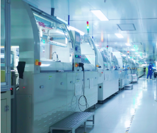
Executing a successful custom LCD display project takes more than just sourcing components off a shelf—it demands tight integration across glass processing, FPC design, surface treatment, and touch calibration. Working with vertically integrated manufacturing partners minimizes supply risks and ensures smooth transitions from initial concept to high-volume production.
Established display specialists like Weitai Technology bring years of custom display engineering experience, in-house optical bonding facilities, advanced SMT lines, and complete quality control systems to complex hardware projects. To discuss technical specifications or explore tailored display module solutions for upcoming hardware builds, visit